#35 Scanning electron microscope & ceramic production
- Definition
- Operating
- Resolution
- Composition and structure of the material
- Examples :
- Surface protection treatments
- Pinholes
- Re-boiling phenomena
1. Definition
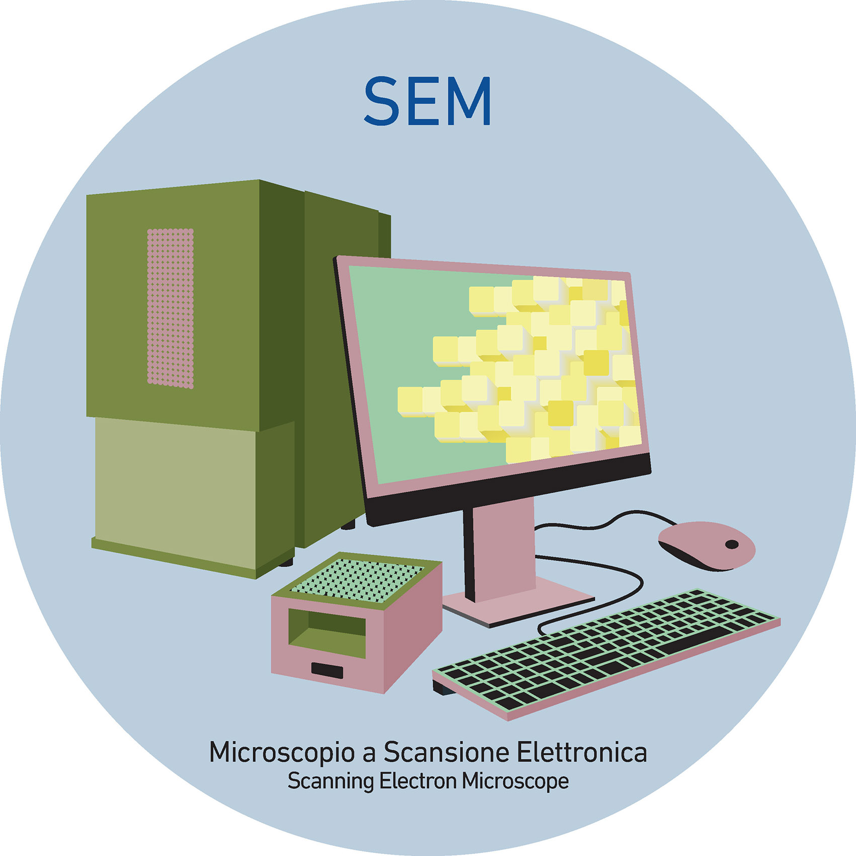
The term SEM is an acronym for Scanning Electron Microscope. This is a high-technological tool that, unlike optical microscopes that take advantage of light as a radiation, makes use of an electronic source (usually tungsten). It is a type of electron microscope that produces images of a sample by scanning the surface with a focused beam of electrons.
This valuable instrument was invented in the 1930s and it is therefore relatively new. The main difference between an optical microscope and an electron microscope is that – to get the image of the surface (in our case a ceramic surface) – the first uses light, while the second uses electrons.
The different source, together with several other benefits, leads to a significant advantage: the analysis is not only about WHAT but also about HOW. The use of electrons, in fact, triggers a series of physical phenomena that can be exploited not only to see the surface but also to deeply understand its composition, how it is made.
2. Operating
What technically happens?
An electron beam is extracted from the source, collimated, and accelerated by the electromagnetic lens system of the electron microscope toward the surface under analysis. The accelerated electrons interact with the first extremely thin layer of the sample’s material, which in turn will emit other electrons. To simplify as much as possible, we can say that the electrons that emerge from the sample and provide the most relevant information are, first, the elastically reflected electrons from the incident beam, which maintain their energy unchanged (primary electrons), and secondly, the electrons ejected from the sample surface due to the inelastic interaction of the electron beam with the surface (secondary electrons). When secondary electrons are emitted from the sample, the latter will be in an excited, high-energy state.
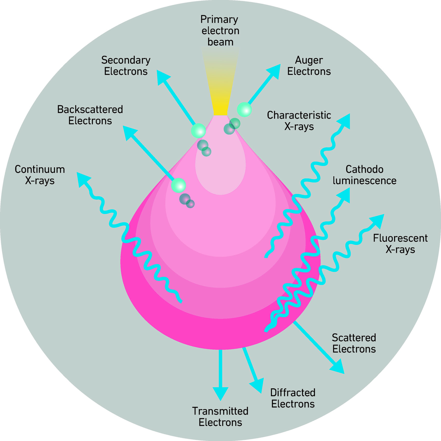
To measure the primary and secondary electrons emerging from the sample without them being annihilated by the atmosphere (destroyed or reduced to nothing), the sample, the electron source, and the tool detectors are housed in a high-vacuum chamber.
Elastic and Inelastic Collision: Definition
If the total mechanical energy of the bodies remains unchanged (and thus the velocities of the two bodies after the collision have different direction, magnitude, or intensity), then it is called an elastic collision. If the mechanical energy of the bodies is partially dissipated during the collision, then it is referred to as an inelastic collision.
What is meant by elastic interaction of the incident electron beam with matter?
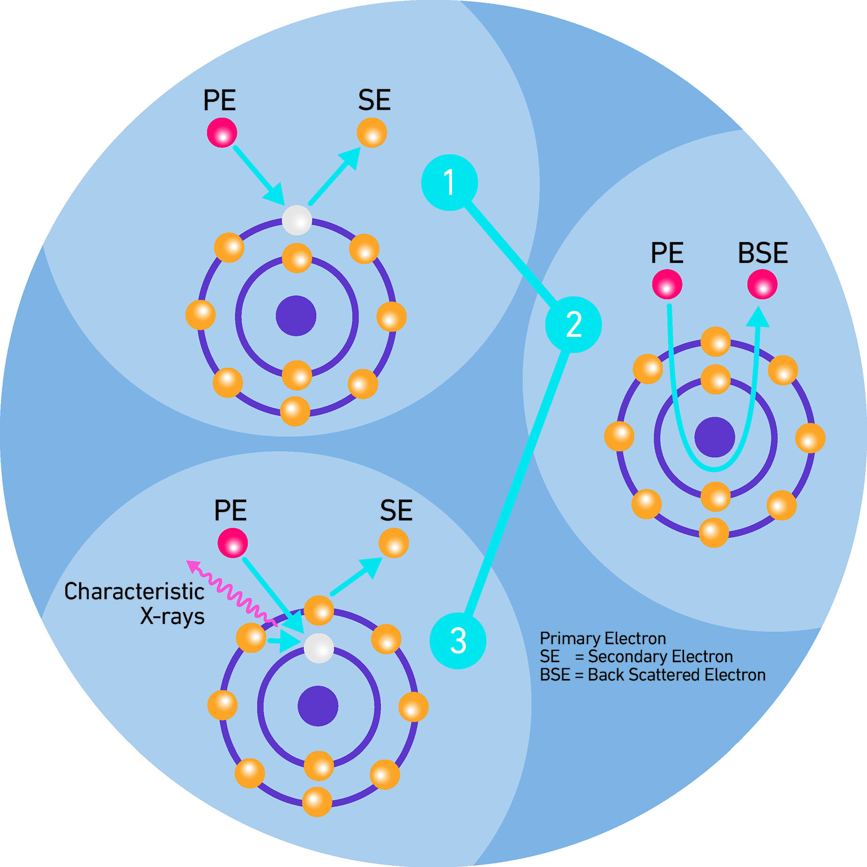
The reflected electrons (backscattered) emerge from the matter with the same energy and can be used to get an image of the sample with which they interacted. The information your reach from these interactions, in addition to morphology, also relates to the density of the matter: the denser the material (heavier atoms), the more likely it is that an elastic interaction will occur with it; conversely, if the material is less dense (lighter atoms), it is less likely that this type of interaction will occur, and fewer electrons will reach the machine’s detectors.
What is the meaning of the inelastic interaction of incident electrons?
Part of the energy of the incident electrons is transferred to the material they collide with. Imagine the electrons bound to the atomic nuclei of the material being literally hit by the electrons of the incident beam. In this process, the incident electrons will transfer some of their energy to the bound electron, which will be ejected. The electrons displaced are called secondary electrons. The material from which these electrons emerge will now be in a state of excitation. The secondary electrons that emerge from the surface can be used by the machine to obtain very high-resolution, three-dimensional images. The process by which the sample’s matter transitions from a high-energy state to a lower one through the emission of X-rays (that change according to each atomic species) allows us to define its composition.
What does all this mean?
Let’s try to translate it into even simpler words.
We can say that a matter in a state of rest is usually marked by a condition of minimal energy and electro-neutrality, meaning a state where the net charge is zero, and each atomic nucleus is surrounded by the corresponding number of electrons bound to it.
The accelerated electrons of the microscope, by removing the electrons from the inner orbitals of the surface atoms, produce an excited state: locally, atoms with an electron-hole are created, meaning a number of electrons lower than initial (or previous) one. This new state of the matter will therefore be at a higher energy compared to the initial electro-neutrality. The atoms in the sample will subsequently tend to return – by their very nature – to a lower energy condition. During the transition between the two states, there will be an emission of energy in the form of X-rays with an energy that correspond to the energetic difference between the two states.
More precisely: most of the electrons discharged from the microscope bounce off the sample, but some possess enough energy to displace part of the electrons present on the surface: the matter will be in a high-energy, unstable state that will tend to evolve into a more stable condition, or at least into a state of lower energy.
It is the excitation (emission of secondary electrons) and de-excitation (emission of X-rays) processes that occur during the interaction between the electrons generated by the microscope and the sample that allow us to determine the atomic composition of the sample that generated and emitted them.
The image is essentially obtained by processing the information deriving from the elastic interactions between the incident beam electrons and the sample surface. In other words, we could say that it is the way the electrons bounce off the sample that generates the image, allowing us to get information and data.
And how does the optical microscope work?
A regular microscope operates based on the laws of optics: light strikes the surface and, by bouncing, enters the lens. Through the phenomenon of diffraction (of light), the image is magnified, and the resolution of the image depends on the wavelength of visible light.
3. Resolution
In terms of resolution, the Scanning Electron Microscope allows for much higher image resolutions, and thus more defined images. Why?
Resolution usually depends on the source used to excite the surface, and in general the smaller the wavelength, the higher the resolution. The source derived from visible light has a wavelength far greater than that of an electron, and thus the optical microscope naturally produces lower-resolution images.
4. Composition and structure of the material
The better resolution, however, is not the only benefit. Along with it, the SEM allows – despite losing information regarding color due to the lack of photon usage – to obtain additional data on the surface composition of the material under analysis.
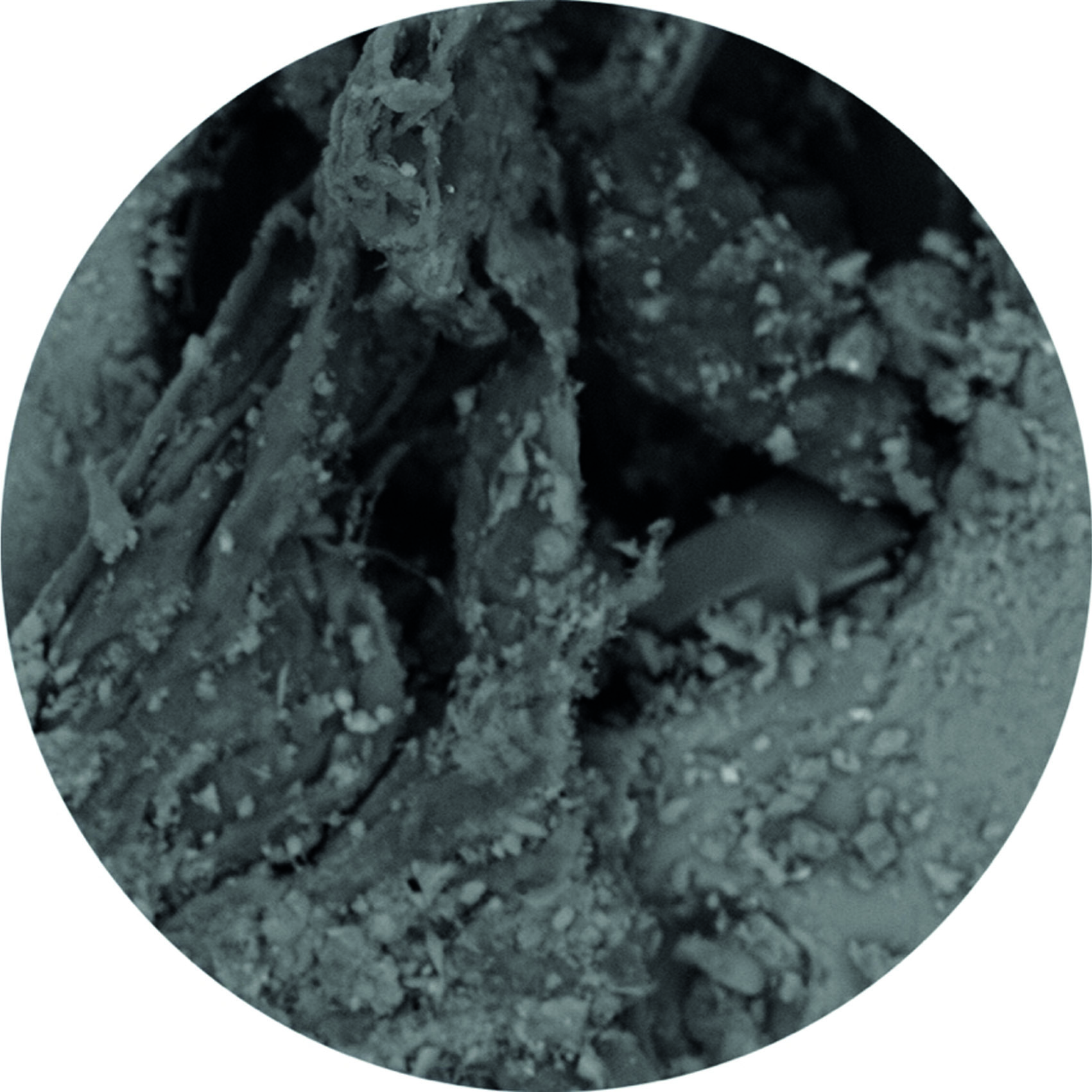
A clear example from the world of ceramics.
Let’s take a surface on which blue digital ink has been applied, then covered with a transparent glaze.
With the naked eye (and with the optical microscope), both the blue color beneath the glaze and the glaze itself are visible, while with the Scanning Electron Microscope, we can detect the composition of the glaze but not that of the dye. This detail reveals a crucial aspect: the optical microscope allows visualization of multiple layers but provides no information regarding material composition, while the Scanning Electron Microscope, though detecting only the surface material (in this case, the glaze), reports in detail the structure of the elements that compose this surface (in this case the glaze).
What happens if the same sample is analyzed in cross-section?
With the SEM, numerous details about the structure and composition of both the glaze and the blue pigment (the interfacing layers) are acquired, while with the optical microscope, only information regarding the morphology can be obtained: in other words, we can verify the presence of different elements without being able to get detail about their composition.
In the case of defects, the action of the scanning electron microscope can, therefore, determine in which layer the defects are located, what generated them, and the composition of the material responsible for the anomaly.
5. Examples
- Example #01: Surface Protection Treatments
Another enlightening example of the different mechanisms of the two types of microscopes can be obtained by addressing the issue of surface protection treatments typically applied to polished tiles to fill the open surface porosity (emerging after polishing or lapping), protecting them from dirt and chemical attacks that could compromise the material over time.
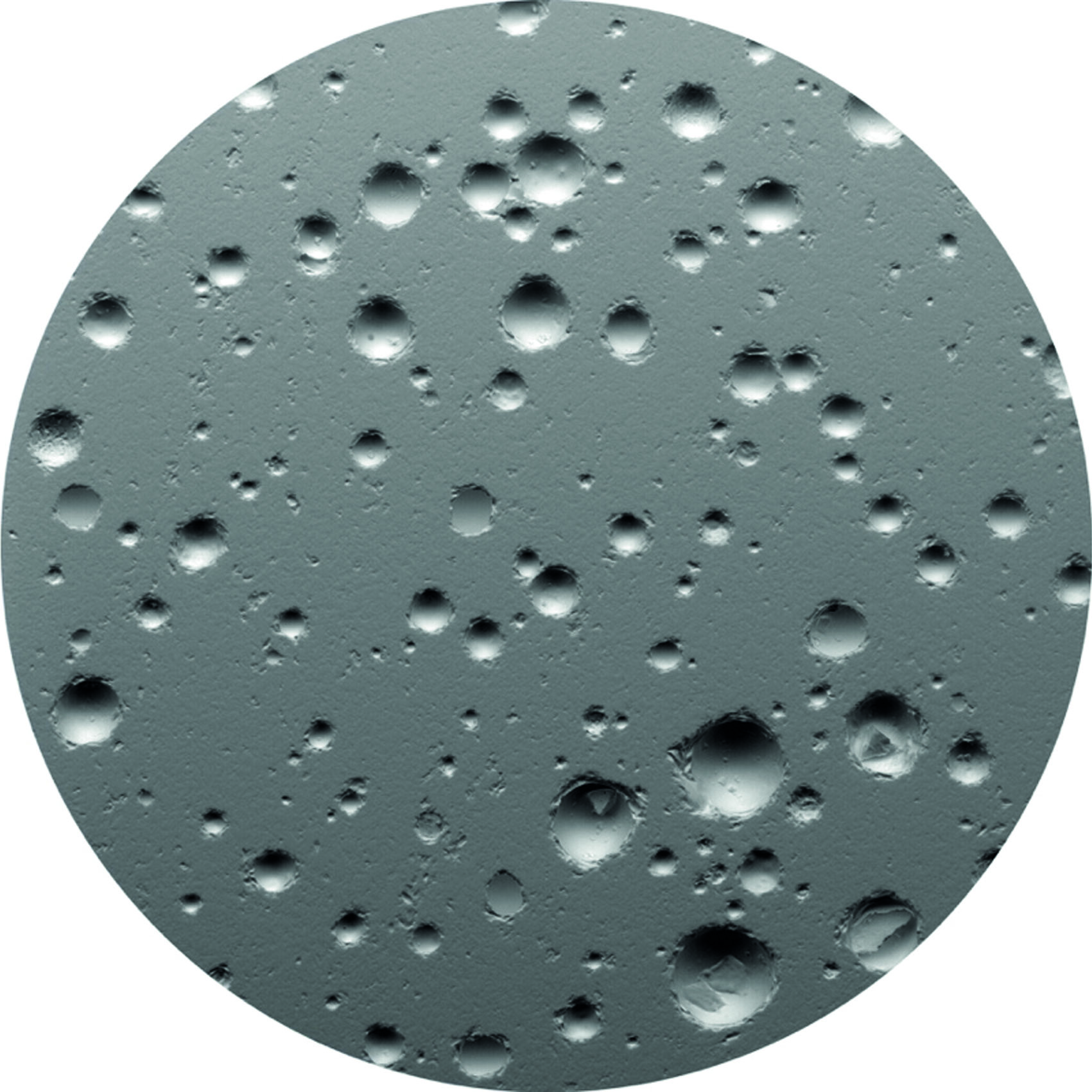
Since the glaze formed after the application is completely transparent, the analysis of the surface using an optical microscope not allow for accurate verification of whether the pores have been properly and fully filled. More precisely: it is possible to infer if the pores are filled, but a reliable indication of their complete and secure filling cannot be obtained. Conversely, the SEM – by returning images of the most superficial part of the sample – allows us to see and measure with extreme precision not only the size of the pores but also to evaluate whether they are fully and correctly filled.
- Example #02: Pinholes
Pinholes are a glaze defect that appear as micro holes on the surface of the tile, and they can penetrate through the surface glaze and the underlying grit, reaching, in extreme cases, even the engobe layer. Pinhole can be formed for several reasons and it can appear from time to time in different positions. For example, in some cases, the defect might originate directly in the pressed support, involving all the overlying layers. In other circumstances, the problem might involve only the engobe and the closest layer. In yet other case the defect could affect only the grit layer.
The scanning electron microscope is essentially capable (by analyzing the sample in cross-section) of accurately identifying the origin of the problem in great detail, thus determining the production phase in which it arose and providing useful guidance on corrective actions that should be implemented.
What does the image of the pinhole look like under the SEM?
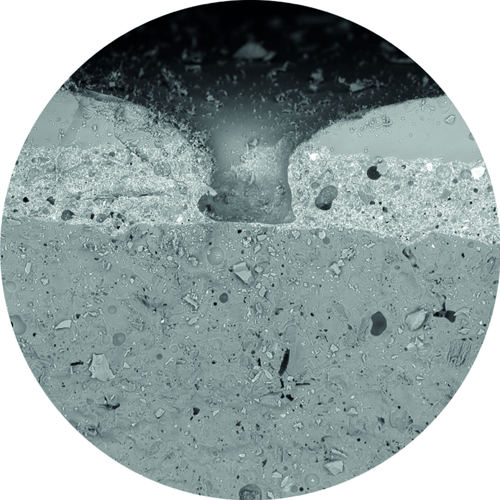
The most important aspect concerns the significant changes in the composition of the material, visible in the cross-section. At the same time, the analysis allows us to delve deeply into the type of variation, such as the presence of very dense materials (usually metals), dissecting their constituent elements in detail.
In this sense, the optical microscope would allow the observation of the morphology (presence and shape) of these intrusions but would not be able to scan the substances that compose them. In some cases, the instrument might not even register the color change promoted by the excess elements.
In other words, for example, in the case of an engobe and a glaze of very similar color, it is challenging to determine where one ends and the other begins. Even if it were possible to identify their different shapes, they would essentially appear the same since their different composition would remain unknown.
On the other hand, with the Scanning Electron Microscope, it is possible to see, for example, the change in composition due to a metallic inclusion that alters the localized fusibility, creating the defect. In this specific case, it will be necessary to trace the origin of the metal: it could be due to a broken sieve or a contaminated raw material.
If this metal cannot be traced, it will be necessary to investigate the formulation of the engobe or the glaze, discovering, for example, the presence of an inappropriate organic content or an excessive amount of wetting agents (which, during firing, can produce overly violent degassing phenomena).
- Example #03: Re-boiling phenomena
Boiling is another type of defect where SEM analysis can be highly effective. It is generally visible to the naked eye, appearing as bubbles trapped inside the glaze / grit in the surface layer of the ceramic body.
Once again, the causes can be numerous and usually overlap, interacting and influencing each other:
- Delayed gas release, which gets trapped when the glaze has already vitrified
- A composition of grit or glaze that is too rich in organic substances, which improperly burn
- Excessive presence of melting elements within the glaze, which causes premature fusion of the solid part
- Interaction with substances (such as inks) that cause the subsequently applied substance to vitrify
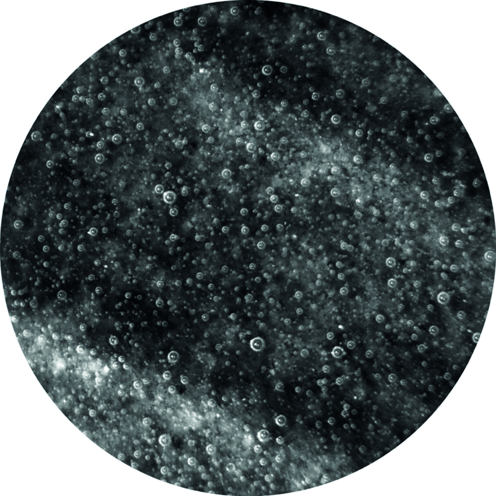
These are just some of the causes, and they are mostly always related to each other. Each of them contributes to making the system unsuitable for the firing cycle set by the manufacturer: the scanning electron microscope allows understanding and unraveling all the cases that may emerge and negatively impact the production process and the final product.